
15. September 2022
GTS CTO Zlatan Stanojević is presenting a novel semi-analytical model for wave-function penetration in MOSFETs, resolving long-standing problems such as carrier spillover and large errors in surface roughness scattering.
A Novel Approach to Modeling Insulator Wave-Function Penetration and Interface Roughness Scattering in MOSFETs
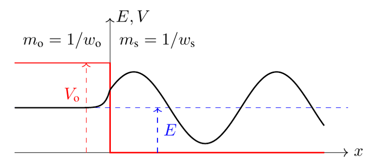
In the paper, Zlatan presents a novel model that allows to consider wave-function penetration into the insulating barrier of MOSFET devices. His analytical penetration model addresses all problems that would emerge when simply including the insulator in the Schrödinger equation, thus providing these advantages:
- No carrier spillover at high inversion or accumulation biases
- Numerically robust wave-function values and their first derivatives at semiconductor/insulator interface and thus stable surface roughness matrix element and mobility
- No mesh density requirements in the insulating barrier, and no additional computational cost with respect to simulations without penetration
Surface Roughness, Numerically Robust
Zlatan further derives an alternative formulation of the surface roughness matrix element that does not require spatial derivatives of the wave-functions and is thus more numerically robust than its textbook counterpart.
The analytical and numerical penetrations converge to the same energies, densities, ψ-values, and roughness-limited mobilities; mobility parameters calibrated without wave-function penetration can be easily recalibrated for the analytical penetration model.
Application: N3+ GAA Devices
Zlatan’s approach is especially apt for highly scaled MOSFET channels and high-barrier dielectrics (such as SiO₂); in his presentation, he discusses applications for N3+ GAA devices.


Paper / Advanced CMOS Modeling Session
| Paper: | ID 6044, topic 3 (presentation 3/3) |
| Session Type: | Lecture |
| Session Code: | A9L-6 |
| Location: | Aula 1d |
| Date & Time: | Tuesday September 20, 2022, 17:30 – 18:30 CEST |
| Chair: | Benjamin Iniguez, Viktor Sverdlov |
ESSDERC/ESSCIRC 2022 session schedule
Update: The paper is available for download here via MyGTS login.
Sensors Device Modeling
Zlatan is also co-chairing the Sensors Device Modeling session:
Sensors Device Modeling Session
| Session Type: | Lecture |
| Session Code: | B2L-5 |
| Location: | Aula 1f |
| Date & Time: | Wednesday September 21, 2022, 09:20 – 10:40 CEST |
| Chair: | Denis Rideau, Zlatan Stanojević |
ESSDERC/ESSCIRC 2022 session schedule
Mentoring Event
Zlatan is acting as a mentor in the Young Professionals and Women in Engineering Mentoring Event:
Young Professionals and Women in Engineering Mentoring Event
| Date & Time: | Tuesday, September 20th, 2022, 13:00 – 14:20 CEST |
| Location: | Aula 10 |